As a Full Professor at the University of Twente’s MESA+ Institute for Nanotechnology I chair an independent research line on quantum electronics within the NanoElectronics group. I am a co-director of the Center for Quantum Nanotechnology Twente (QUANT), and coordinator of the Horizon Europe project ONCHIPS. You can find a relatively technical description or my research here. These videos are reasonably accessible for a broader audience: ONCHIPS, TOPSQUAD and QUANT. Here are a Dutch radio interview and podcast about Quantum physics and technology (Sep 2021).
CURRICULUM VITAE
Full Professor of Quantum Electronics, University of Twente (2022–present).
Director Center for Quantum Nanotechnology Twente (QUANT), (2020–present).
Associate Professor, University of Twente (2015–2021).
Assistant Professor, University of Twente (2011–2015).
Field of research: Quantum Electronics
Post-doc, UNSW Sydney, Australia (2008–2011).
PIs: Andrew Dzurak, Andrea Morello
PhD, TU Delft (2008). Advisor: Leo Kouwenhoven.
Thesis: Spin and charge in semiconductor nanowires
Visiting Scientist, Harvard University, USA (2003).
PI: Charles Marcus
MSc Applied Physics, TU Delft, NL (2003).
Thesis supervisor: Hans Mooij
PUBLICATIONS
40 publications, >3400 citations, h = 23. (Web of Science)
GRANTS AND AWARDS
2025 – ERC SYNERGY GRANT (European Research Council)
2023 – VICI laureate (Dutch Science Foundation NWO)
2023 – NGF Quantum Technology (Dutch Science Foundation NWO)
2020 – FET-FLAG (European Commission H2020)
2020 – ENW Groot (Dutch Science Foundation NWO)
2019 – FET-OPEN coordinator (European Commission)
2017 – NWA Startimpuls (Dutch Science Foundation NWO)
2015 – VIDI laureate (Dutch Science Foundation NWO)
2015 – Prize for excellent teaching in BSc Advanced Technology
2013 – FET ProActive (European Commission FP7 Program)
2012 – FOM Projectruimte (Foundation for Fundamental Research on Matter)
2011 – VENI laureate (Dutch Science Foundation NWO)
2011 – Marie Curie career Integration Grant (European Commission)
2011 – NWO nano (Dutch Science Foundation NWO)
OPEN POSITIONS
Throughout the year we have a few PhD and Post-doc positions available in our group. Starting April 2025 we have an open post-doc position and several PhD positions. Open applications are welcome at any time. You may directly contact me for more information.
Organisations
In the field of silicon quantum electronics we study the quantummechanical behavior of individual spins in silicon. Control and manipulation of the corresponding spin states can be lead to applications in quantum computation. To this end we isolate electrons or holes on (artificial) atoms through spatial and electrostatic confinement. In our experiments we perform a.o. energy- and magnetic spectroscopy in electron transport measurements at low temperatures.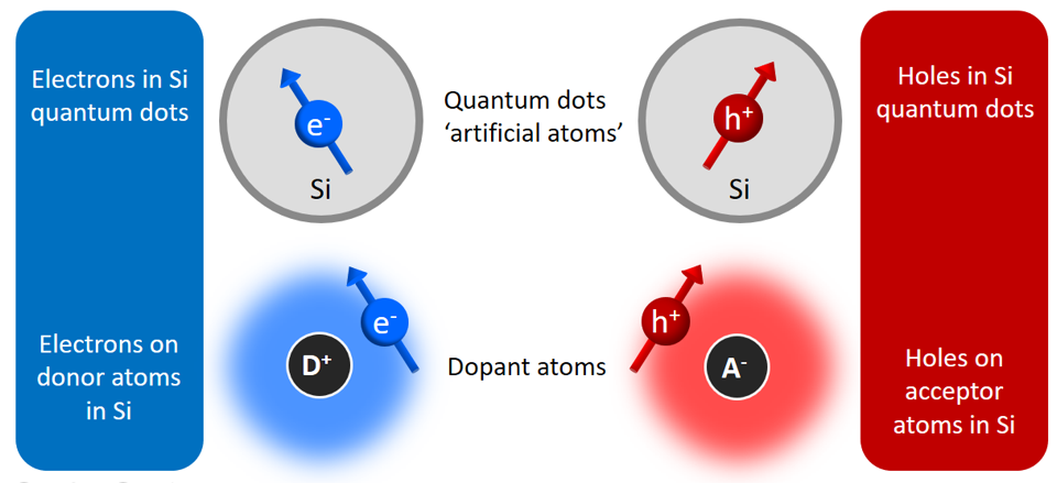
Four approaches to study single spins in silicon: we isolate individual electrons and holes, either in real or artificial atoms.
Click here for a direct link to our publications.
Single electron spins as quantum bits
Among other proposed physical realizations for quantum information processors, semiconductor-based qubits belong to the most popular suggestions. In particular, electron spins in quantum dots (QDs) have received considerable attention, and significant experimental progress has been made since Loss and DiVincenzo presented their original proposal, see Phys. Rev. A 57, 120 (1998). Experiments on lithographically defined QDs in GaAs/AlGaAs heterostructures have shown qubit initialization, single-shot single-electron spin read-out, and coherent control of single-spin and two-spin states. The strong hyperfine and spin-orbit interaction in AlGaAs/GaAs QDs limit the spin coherence time in those materials. In silicon, extremely long spin relaxation (T1) and coherence times (T2) are expected. Recently, a direct measurement was performed of the T1 of a single electron in silicon, which is ~6 seconds at a magnetic field of 1.5 Tesla, see Nature 467, p. 687 (2010).
Spin qubits in silicon quantum dots
We aim at controlling the spin states of individual electrons in silicon double quantum dots (DQDs) with the ultimate goal of realizing silicon single-electron spin quantum bits as building blocks for future solid-state quantum computers, see e.g. Nature 464, 45-53 (2010). Although important progress has been made over the last few years, it is not trivial to define QDs in Si. The main issues are the large effective mass of the charge carriers and the sensitivity to disorder, resulting in carrier localization on short length scales, and thus multiple QDs connected in series. The most successful systems for n-Si QDs are etched silicon-on-insulator structures, two-dimensional electron gases in Si/SiGe heterostructures and at Si/SiO2 interfaces (planar quantum dots), and bottom-up grown nanowires.
In the NanoElectronics group we use two material systems to isolate single electron and hole spins in Si QDs:
Ambipolar planar Si quantum dots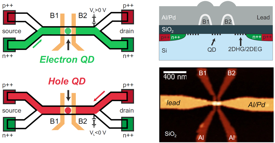
Ge/Si nanowire quantum dots 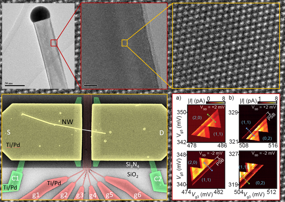
Ge/Si nanowire quantum dots
These semiconducting crystalline nanowires, with aspect ratios of 1000 or more, have diameters up to tens of nanometers and can be tens of microns long. Their strength lies in the precisely controlled and tunable chemical composition, structure, size, and morphology. The high degree of freedom in nanowire synthesis allows epitaxial growth of heterostructures in both the radial and longitudinal direction. The doping in nanowires can be varied during growth, to make for example pn-junctions within a single nanowire to create LEDs.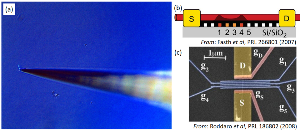 Nanowire quantum dots.(a) Microscope image of a Ge nanowire sticking to the tip of our micromanipulator. Ge, Si and Ge/Si nanowires are grown at Eindhoven University by the Vapor-Liquid-Solid growth mechanism, see here. After synthesis the nanowires are deposited on an oxidized silicon substrate with predeposited bottom gates. In a subsequent fabrication step, source (S) and drain (D) contacts are evaporated on top of the nanowire, see (b) for a schematic cross-section and (c) for a top view of a real device. Voltages applied to the bottom gates are used to create a quantum dot, and control both charge occupation and tunnel barriers.
Highly tunable planar Si quantum dots compatible with CMOS industry
We define Si QDs in an electron or hole gas at the Si/SiO2 interface through electrostatic gating. See for example our recent report on “Single-hole tunneling through a two-dimensional hole gas in intrinsic silicon”, P.C. Spruijtenburg, J. Ridderbos, F. Mueller, A. W. Leenstra, M. Brauns, A. A. I. Aarnink, W. G. van der Wiel & F. A. Zwanenburg, Applied Physics Letters 102, 192105 (2013). The n-type version is described here: “Observation of the single-electron regime in a highly tunable silicon quantum dot”, W. H. Lim, F. A. Zwanenburg, H. Huebl, M. Möttönen, K. W. Chan, A. Morello, and A. S. Dzurak Appl. Phys. Lett. 95, 242102 (2009).
The design with three layers of gates allows control of all QD components: the QDs themselves, the tunnel barriers and the densities of states in the reservoirs. In collaboration with the group of Prof. Dzurak at the University of New South Wales, we are further developing the Si QD technology towards few-electron double quantum dot devices, see figure below.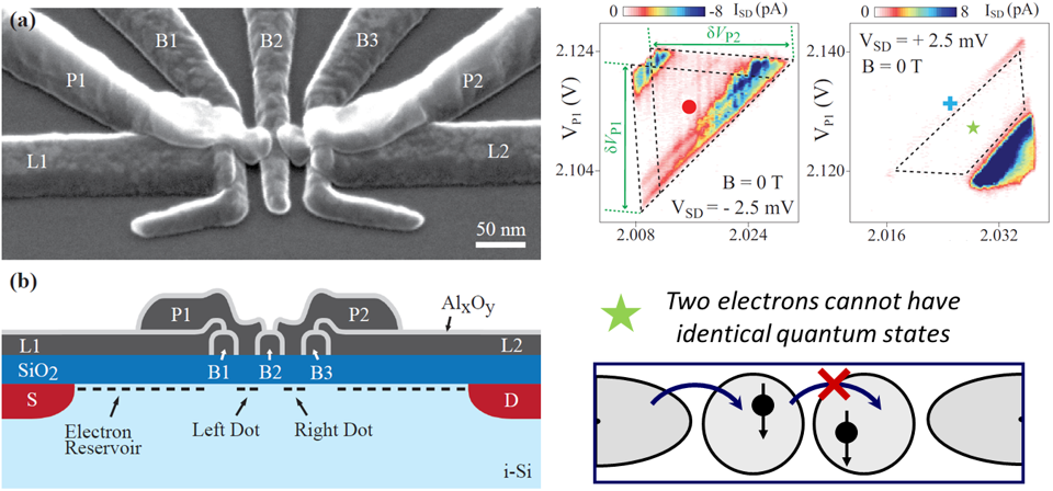 Pauli spin blockade in a many-electron Si metal-oxide-semiconductor (MOS) double QD. (a) Scanning electron micrograph (SEM) image of a highly tunable single electron Si/SiO2 DQD. (b) Schematic cross section of the Si MOS double quantum dot. The architecture is defined by barrier gates B1, B2 and B3, lead gates L1 and L2, and plunger gates P1 and P2. The gates are separated by an Al2O3 layer (light gray). (Right boxes) At positive bias the current is fully suppressed by spin blockade (green star box). Figures from Scientific Reports 1, 110, (2011).
Spin blockade in few-electron Si double quantum dots
The number of electrons (m,n) on the left (m) and right (n) QD can be reduced by decreasing the gate voltages, but then the tunnel barriers become less transparent and currents too low to measure. Due to the tunability of this device we are able to counteract the loss of barrier transparency by increasing the barrier gate voltages, resulting in a measurable current through the QD down to the last electron in both QDs.
After having found the (0,0) regime in transport, it is straightforward to move to the (1,1) « (0,2) transition. Here, Pauli spin blockade manifests itself: transport will always be possible from (0,2) to (1,1), no matter whether the (0,2) forms a triplet (T) or a singlet-state (S), see Figure above. However, when the bias voltage is reversed, transport will be impossible at low bias due to Pauli spin blockade: If the (1,1) state is a singlet, an electron can tunnel through via the (0,2) singlet-state. However, if the (1,1) state is a triplet-state, transport will be blocked since the (0,2) triplet-state is much higher in energy and a transition from T(1,1) to S(0,2) would require a spin-flip.
Coherent single electron spin resonance
Spin blockade in a highly tunable double QD system opens the pathway to the rotation of an electron spin into a superposition of spin-up and spin-down. Spin blockade has been combined with an AC magnetic field to perform ESR on a single electron spin in a AlGaAs/GaAs quantum dot. The spin blockade is then lifted by rotating individual electron spins at an experimentally controlled frequency. We want to use this scheme to measure the spin coherence time T2 in Si. The logical next step is to realize driven coherent oscillations of electron spins induced by microwave bursts, a basic requirement for quantum information processing with single electron spins.
---------------------------------------------------------------------------------------------------
The Silicon Quantum Electronics team 2017
Sergey Amitonov (Post-doc)
Joost Ridderbos (PhD student)
Alejandro Márquez Seco (PhD student)
Jeroen van Gelder (MSc student)
Bram van de Ven (MSc student)
Thijs van den Berg (MSc student)
Wilfred van der Wiel (Full Professor)
Floris Zwanenburg (Associate Professor)
Alumni
Dr. Filipp Müller
Dr. Matthias Brauns
Dr. Paul-Christiaan Spruijtenburg
Anne Leenstra MSc
Georgios Konstantaras MSc
Joren van Kempen MSc
Reinier Nielen MSc
Yizhen Ren MSc
Joost van der Hoff MSc
Agung Sriwongo MSc
Ton Nguyen MSc
Florian Bruijnes MSc
Gertjan Eenink MSc
Max Vervoort MSc
William Elferink BSc
Abla Al-Kiyumi BSc
Fotis Avgidis BSc
Collaborations, past and present
- Eindhoven University: Erik Bakkers, Ang Li, Yizhen Ren
- Delft University: Leo Kouwenhoven, Menno Veldhorst, Giordano Scappucci, Sonia Conesa-Boj
- University of New South Wales: Andrew Dzurak, Andrea Morello, Wee Han Lim, Dimi Culcer
- University of Basel: Daniel Loss, Jelena Klinovaja, Dominik Zumbühl, Floris Braakman, Florian Froning
- CEA Grenoble: Xavier Jehl, Marc Sanquer
- IBM Research Zürich: Andreas Fuhrer
For more information, please contact Floris Zwanenburg (f.a.zwanenburg@utwente.nl_ - remove underscore before sending message).
THE LINK BELOW IS AUTOMATICALLY GENERATED BY THE UNIVERSITY WEBSITE AND IS INCOMPLETE. FOR A COMPLETE LIST OF PUBLICATIONS CLICK HERE.
Research profiles
Affiliated study programs
Courses academic year 2026/2027
Courses in the current academic year are added at the moment they are finalised in the Osiris system. Therefore it is possible that the list is not yet complete for the whole academic year.
Courses academic year 2025/2026
Courses academic year 2024/2025
In the press
- A Dutch Radio1 interview and corresponding podcast about Quantum physics and technology (Sep 2021).
- These two videos are reasonably accessible for a broad audience: FET-OPEN project TOPSQUAD and our Centre for Quantum Nanotechnology Twente QUANT.
- For experts: a relatively technical description of my research on silicon quantum electronics.
Address

University of Twente
Carré (building no. 15), room C1435
Hallenweg 23
7522 NH Enschede
Netherlands
University of Twente
Carré C1435
P.O. Box 217
7500 AE Enschede
Netherlands
 Scan the QR code or